My Learning Journey - PCB Design with KiCad
From schematic diagrams to circuit board layout and practical projects.
← Back to PortfolioDay 1
KiCadSchematic Diagrams & KiCad Installation
My PCB design journey started with the fundamentals: understanding **schematic diagrams** and setting up my design environment. I installed and configured **KiCad**, an open-source EDA suite, and learned how to use its **schematic editor** to create a blueprint of an electronic circuit. This day was crucial for grasping how components are represented and connected before any physical layout begins.
Key Learnings:
- Understanding the purpose and components of a schematic diagram.
- Installing and configuring KiCad for a new project.
- Using the KiCad schematic editor to place components and draw nets.
- Annotating components and performing an Electrical Rules Check (ERC).

Creating the circuit's blueprint in KiCad's schematic editor.
Day 2
KiCad ProjectDesigning an AC-to-AC Converter
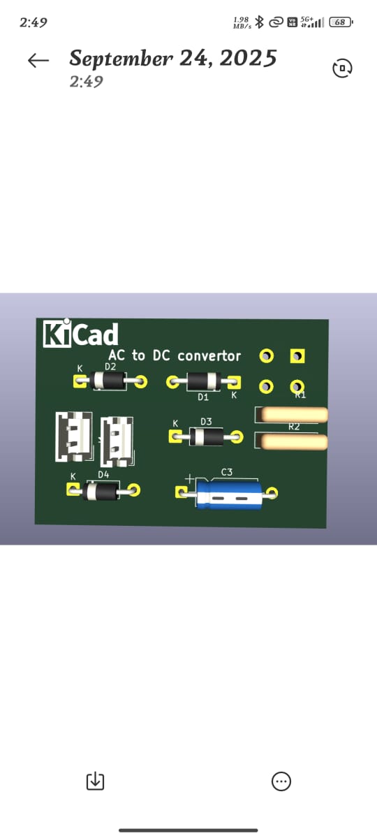
I applied my newfound skills to a practical project: designing a PCB for an **AC-to-AC converter**. I transitioned from the schematic to the **PCB layout editor** in KiCad. This hands-on experience taught me how to place components, route copper traces, and use the **3D viewer** to inspect the design. This project highlighted the importance of proper component placement and trace routing for a functional and manufacturable board.
Project Steps & Skills Developed:
- Creating a netlist and importing it into the KiCad PCB editor.
- Placing components on the board and routing copper traces.
- Running Design Rules Check (DRC) to find errors.
- Using the 3D viewer to check for physical fit and clearance.
- Generating Gerber files for fabrication.
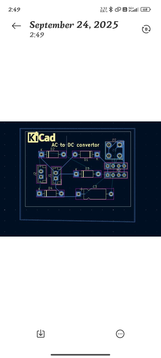
Laying out and visualizing the AC-to-AC converter PCB in 3D.
Day 3
KiCad ProjectDC Motor Speed Controller
On the final day, I tackled a more complex project: a **DC motor speed controller**. This project required careful consideration of power and signal traces. I learned about **Pulse Width Modulation (PWM)** and how to route power-carrying traces to be wider and separate them from sensitive signal lines to prevent interference. This project was a great way to consolidate my KiCad skills on a real-world, functional circuit.
Project Steps & Skills Developed:
- Designing the schematic for a DC motor speed controller.
- Implementing PWM in the circuit design.
- Applying advanced routing techniques for power and signal lines.
- Generating manufacturing files, including Gerber and drill files.
- Final review and documentation of the design.
Designing the PCB for a motor speed controller.